Stanford University, TechConnect World-National Innovation Summit 2013 Participant, Washington, DC
Chi Hwan Lee, a [leading] researcher at Stanford University, recently discussed their invention of the Peel-and-Stick process presented at the TechConnect World-National Innovation Summit. Lee explained, “The technology is a manufacturing technique that can peel off the fully fabricated, thin-film electronics, such as thin-film transistors and solar cells, from its fabrication substrate to arbitrary substrates, such as papers, plastics, etc.”
The invention, [a] Peel-and-Stick process, transfers thin-film electronic devices (prefabricated on rigid, opaque and brittle Si wafer) to diverse unusual, yet useful substrates such as paper, plastics, tapes, glasses, and metal foils. This then impacts a wide range of technologies, including flexible, cheap and light-weight displays, solar cells, and bio-integrated thin-film electronics.
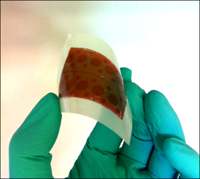
The thin-film electronic devices are pre-fabricated on a SiO2/Si wafer with a ductile metal layer (i.e., Cu, Al, Ni) by using conventional fabrication methods such as photo and electron beam lithography. A temporary holder, such as thermal release tape, is attached to the top of the substrate, and then the whole structure is soaked in water at room temperature, followed by a peel-off of the temporary holder. During the peel-off process, the water can quickly penetrate into the interface between the metal and SiO2 layers because of the environmental-assisted subcritical debonding phenomenon. Consequently, the thin-film electronic devices are detached from the Si wafer and sandwiched between the temporary holder and metal layers. The metal layer can be etched away by the appropriate metal etchant if necessary. Lastly, the thin-film electronic device is pasted onto the target substrate, and the temporary holder is released. Note that a thin glue layer, such as polydimethylsiloxane(PDMS), polyvinyl alcohol (PVA) can be pre-coated on non-adhesive target substrates. Most importantly, the electrical performances of the thin-film electronic devices are identical before and after the Peel-and-Stick process.
Xiaolin Zheng, professor of mechanical engineering at Stanford University, leads the team of researchers. Recently, Dr. Zheng was honored as one of the innovators among the 100 Leading Global Thinkers by the Foreign Policy Magazine, and also recognized on the 2013 TR35 Global list by MIT Technology Review. TR35 recognizes a list of 35 exceptionally talented technologists under the age of 35, whose potential work could transform the world. For further information on Dr. Zheng’s achievements, please visit: http://www.foreignpolicy.com/2013_global_thinkers/public/zheng
http://www.technologyreview.com/lists/innovators-under-35/2013/pioneer/xiaolin-zheng/
We asked Dr. Lee where the technology currently stands, and he told us: “The technology is scalable and we believe manufacturable. Currently, a related patent is pending.” Over the next year, the team hopes to build an automatic peeler over large areas, such as roll-to-roll system. For the demonstrations at the present stage, the thin-film electronic devices are peeled by hand.
The team at Stanford University is searching for partnering and funding opportunities.
For further information about the technology, please view the following presentation: http://www.youtube.com/watch?v=O3xvjz9iYE4 or contact Chi Hwan Lee via email at clee58@stanford.edu
Subscribe to our mailing list, and we'll keep you posted of the latest developments.

 RSS feed of TechConnect News™